
Maxim Ziatdinov, Rama Vasudevan, Sergei Kalinin
Oak Ridge National Laboratory
Introduction
Scanning Probe and Electron microscopes are the tools that opened the atomic world for exploration by providing the beautiful images of metals, oxides, semi- and superconductors with atomic resolution. Currently, both the scanning probe and transmission electron microscopy (SPM and STEM) fields almost invariably rely on classical rectangular raster scans in which the beam or the probe rapidly traverses the surface in the fast scan direction, and slowly shifts in the perpendicular direction forming the slow scan direction. This scanning mode offers both the advantage of easy implementation and yields data in the form of 2D maps that can be readily interpreted by a human eye.
However, the rectangular scanning is inefficient from the information theory point of view, since the interesting information is often concentrated in a small number of regions on the sample surface. Hence, beyond rectangular scanning becomes a key prerequisite for the AE aimed at structural discovery, minimizing the surface damage, or attempting controlled modification of the surface. The possible paradigms for AE in this case are summarized in Figure 1. Ultimately, we can envision the freeform scanning approaches, where the direction and velocity of the probe motion are updated based on previously detected information. However, given the latencies of SPM and STEM imaging, this will necessitate development of specialized light algorithms and edge computations, as discussed below. On a shorter time frame, adapting the parameters of the predefined waveform, e.g., pitch of the spiral or line density in rectangular sub scans offers a more practical alternative.
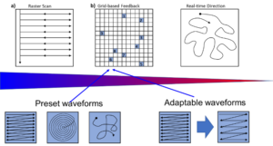
Figure 1. Possible scanning paradigms in SPM and STEM. Shown are (a) classical scan, (b) sub-scan-based images for structural discovery, based either on preset or adjustable scan-forms, or (c) freeform scanning. The selection of image regions in (b) or scanning direction and velocity in (c) are guided by a suitable ML algorithm.
Dataset
‘Graphene_CrSi.npy’ contains a scanning transmission electron microscopy (STEM movie from graphene monolayer. The movie is a sequence of atom-resolved images from the same sample region that undergoes chemical and structural transformations due to interaction with electron beam (which is used to perform imaging). ‘topo_defects.npy’ contains coordinates of some of the objects of interest (topological defects in graphene). It is a dictionary, where keys are frame numbers and values are xy coordinates. These objects are usually localized in relatively small areas of the image and we are interested in identifying them without having to scan an entire grid (which leads to fast degradation of the sample).
The dataset can be accessed at https://doi.ccs.ornl.gov/ui/doi/326.
Challenge Questions
The challenges are:
 Download
 Slack Channel
 Challenge Contact
 Dataset