This challenge is driven by efforts in Scanning Transmission Electron Microscopy to expedite materials data analysis, and generate insight into physics and chemistry of 2D materials irradiated by the electron beam.
Scanning transmission electron microscopy (STEM) and associated spectroscopies are well established, robust imaging tools that have proved to be powerful in visualization of structure and functionality of materials with atomic resolution.1 2 The ultimate goal of localized imaging and spectroscopy is to observe and quantitatively correlate structure-property relationships with functionality – by evaluating chemical, electronic, optical and phonon properties of individual atomic and nanometer-sized structural elements.3 Historic improvements in the underlying instrument hardware and data processing technologies has allowed determination of atomic positions with sub-10 pm precision4, 5 which enabled the visualization of chemical and mechanical strains,6 and order parameter fields including ferroelectric polarization7-10 and octahedral tilts.11-15 Ideally, complete studies have to be performed as a function of global stimuli, such as temperature or uniform electric field applied to the system, as well as local stimuli that are induced by additional electron probe interactions.16-18 Furthermore, this technical combinatorial instrumentation challenge is exacerbated by a wealth of extracted information at both global and local scales necessitating a drastic improvement in capability to transfer, store and analyze multidimensional data sets.
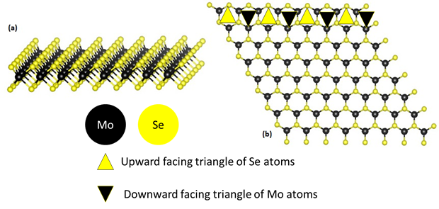
In this challenge, contestants will be supplied with a short atomically resolved movie, 49 individual frames, which illustrate MoSe2 film evolution under the electron beam. We are interested in the motion of the Mo and Se atoms captured throughout the movie. The positions of the atoms and their trajectory will serve as inputs to a Density Functional Theory simulation to reveal the details of the beam-matter interaction, as well as material reconstruction and vacancy formation mechanisms associated with beam induced stress.
1. Pennycook, S. J.; Nellist, P. D., Scanning Transmission Electron Microscopy: Imaging and Analysis. Springer: New York, 2011.
2. Pennycook, S. J.; Chisholm, M. F.; Lupini, A. R.; Varela, M.; van Benthem, K.; Borisevich, A. Y.; Oxley, M. P.; Luo, W.; Pantelides, S. T., Materials Applications of Aberration-Corrected Scanning Transmission Electron Microscopy. In Advances in Imaging and Electron Physics, Vol 153, Hawkes, P. W., Ed. Elsevier Academic Press Inc: San Diego, 2008; Vol. 153, pp 327-+.
3. Mody, C., Instrumental Community: Probe Microscopy and the Path to Nanotechnology. MIT Press: 2011.
4. Yankovich, A. B.; Berkels, B.; Dahmen, W.; Binev, P.; Sanchez, S. I.; Bradley, S. A.; Li, A.; Szlufarska, I.; Voyles, P. M., Picometre-Precision Analysis of Scanning Transmission Electron Microscopy Images of Platinum Nanocatalysts. Nature Communications 2014, 5.
5. Kim, Y. M.; He, J.; Biegalski, M. D.; Ambaye, H.; Lauter, V.; Christen, H. M.; Pantelides, S. T.; Pennycook, S. J.; Kalinin, S. V.; Borisevich, A. Y., Probing Oxygen Vacancy Concentration and Homogeneity in Solid-Oxide Fuel-Cell Cathode Materials on the Subunit-Cell Level. Nature Materials 2012, 11, 888-894.
6. Kim, Y. M.; Morozovska, A.; Eliseev, E.; Oxley, M. P.; Mishra, R.; Selbach, S. M.; Grande, T.; Pantelides, S. T.; Kalinin, S. V.; Borisevich, A. Y., Direct Observation of Ferroelectric Field Effect and Vacancy-Controlled Screening at the Bifeo3/Laxsr1-Xmno3 Interface. Nature Materials 2014, 13, 1019-1025.
7. Chang, H. J.; Kalinin, S. V.; Morozovska, A. N.; Huijben, M.; Chu, Y. H.; Yu, P.; Ramesh, R.; Eliseev, E. A.; Svechnikov, G. S.; Pennycook, S. J., et al., Atomically Resolved Mapping of Polarization and Electric Fields across Ferroelectric/Oxide Interfaces by Z-Contrast Imaging. Advanced Materials 2011, 23, 2474-+.
8. Nelson, C. T.; Winchester, B.; Zhang, Y.; Kim, S. J.; Melville, A.; Adamo, C.; Folkman, C. M.; Baek, S. H.; Eom, C. B.; Schlom, D. G., et al., Spontaneous Vortex Nanodomain Arrays at Ferroelectric Heterointerfaces. Nano Letters 2011, 11, 828-834.
9. Jia, C. L.; Nagarajan, V.; He, J. Q.; Houben, L.; Zhao, T.; Ramesh, R.; Urban, K.; Waser, R., Unit-Cell Scale Mapping of Ferroelectricity and Tetragonality in Epitaxial Ultrathin Ferroelectric Films. Nature Materials 2007, 6, 64-69.
10. Jia, C. L.; Urban, K. W.; Alexe, M.; Hesse, D.; Vrejoiu, I., Direct Observation of Continuous Electric Dipole Rotation in Flux-Closure Domains in Ferroelectric Pb(Zr,Ti)O(3). Science 2011, 331, 1420-1423.
11. Jia, C. L.; Mi, S. B.; Faley, M.; Poppe, U.; Schubert, J.; Urban, K., Oxygen Octahedron Reconstruction in the Srtio(3)/Laalo(3) Heterointerfaces Investigated Using Aberration-Corrected Ultrahigh-Resolution Transmission Electron Microscopy. Physical Review B 2009, 79.
12. Kim, Y. M.; Kumar, A.; Hatt, A.; Morozovska, A. N.; Tselev, A.; Biegalski, M. D.; Ivanov, I.; Eliseev, E. A.; Pennycook, S. J.; Rondinelli, J. M., et al., Interplay of Octahedral Tilts and Polar Order in Bifeo3 Films. Advanced Materials 2013, 25, 2497-2504.
13. Borisevich, A. Y.; Chang, H. J.; Huijben, M.; Oxley, M. P.; Okamoto, S.; Niranjan, M. K.; Burton, J. D.; Tsymbal, E. Y.; Chu, Y. H.; Yu, P., et al., Suppression of Octahedral Tilts and Associated Changes in Electronic Properties at Epitaxial Oxide Heterostructure Interfaces. Physical Review Letters 2010, 105.
14. He, J.; Borisevich, A.; Kalinin, S. V.; Pennycook, S. J.; Pantelides, S. T., Control of Octahedral Tilts and Magnetic Properties of Perovskite Oxide Heterostructures by Substrate Symmetry. Physical Review Letters 2010, 105.
15. Borisevich, A.; Ovchinnikov, O. S.; Chang, H. J.; Oxley, M. P.; Yu, P.; Seidel, J.; Eliseev, E. A.; Morozovska, A. N.; Ramesh, R.; Pennycook, S. J., et al., Mapping Octahedral Tilts and Polarization across a Domain Wall in Bifeo(3) from Z-Contrast Scanning Transmission Electron Microscopy Image Atomic Column Shape Analysis. Acs Nano 2010, 4, 6071-6079.
16. Chang, H. J.; Kalinin, S. V.; Yang, S.; Yu, P.; Bhattacharya, S.; Wu, P. P.; Balke, N.; Jesse, S.; Chen, L. Q.; Ramesh, R., et al., Watching Domains Grow: In-Situ Studies of Polarization Switching by Combined Scanning Probe and Scanning Transmission Electron Microscopy. Journal of Applied Physics 2011, 110, 052014.
17. Nelson, C. T.; Gao, P.; Jokisaari, J. R.; Heikes, C.; Adamo, C.; Melville, A.; Baek, S. H.; Folkman, C. M.; Winchester, B.; Gu, Y. J., et al., Domain Dynamics During Ferroelectric Switching. Science 2011, 334, 968-971.
18. Belianinov, A.; Iberi, V.; Tselev, A.; Susner, M. A.; McGuire, M. A.; Joy, D.; Jesse, S.; Rondinone, A. J.; Kalinin, S. V.; Ovchinnikova, O. S., Polarization Control Via He-Ion Beam Induced Nanofabrication in Layered Ferroelectric Semiconductors ACS Nano 2015, Under Review.